

Australia’s CSIRO has achieved a significant breakthrough, demonstrating the power of quantum machine learning in semiconductor design. Their work, published in a recent study, showcases how a quantum-enhanced model can outperform conventional artificial intelligence methods, potentially reshaping the future of microchip fabrication. The core of their innovation lies in accurately modeling “Ohmic contact” resistance, a critical property that dictates how efficiently current flows between a metal contact and a semiconductor material.
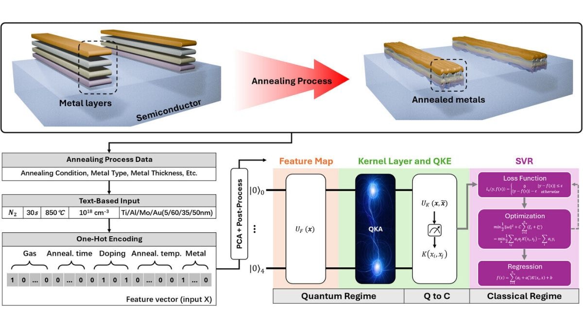
The team focused their efforts on advanced gallium nitride (GaN) transistors, known for their high-power and high-frequency capabilities. They analyzed data from 159 experimental samples, using a hybrid quantum-classical approach. By integrating a quantum processing layer with a classical regression step, the model was able to discern subtle patterns that had eluded traditional analytical methods. This could lead to faster, more efficient microchip designs.
The complexity of semiconductor fabrication lies in the sheer number of variables involved. Factors such as gas mixtures, annealing times, and deposition rates all influence the final performance of the chip. Modeling these interactions using conventional methods can be extremely challenging. However, CSIRO’s approach offers a new perspective, potentially unlocking more efficient and powerful designs.
- Quantum-enhanced model outperforms classical AI.
- Focus on modeling Ohmic contact resistance in GaN transistors.
- Hybrid quantum-classical approach enables pattern recognition.
- Validated with fabricated devices showing improved performance.
The researchers, led by Professor Muhammad Usman, first tackled the challenge of data dimensionality. They initially encoded 37 different fabrication parameters for each device. Recognizing the limitations of current quantum hardware, they employed principal component analysis (PCA) to reduce this to the five most influential parameters. As Professor Usman explained, “The quantum computers that we currently have very limited capabilities. We needed to distill the problem to its essence.”
Classical machine learning algorithms often struggle with datasets that are both limited in size and characterized by non-linear relationships. By focusing on the most crucial variables, the CSIRO team created a problem that was manageable for existing quantum computers, while still retaining the complexity needed to accurately model the system.
Their quantum kernel-aligned regressor (QKAR) architecture is at the heart of the innovation. The five key parameters for each sample were mapped onto a five-qubit quantum state using a Pauli-Z feature map. This enabled the quantum kernel layer to effectively capture complex correlations within the data. The output from this quantum layer was then fed into a standard learning algorithm, which identified the manufacturing parameters that had the most significant impact on performance. According to Usman, this combined quantum-classical model makes it possible to pinpoint which fabrication steps should be fine-tuned to achieve optimal device performance.
Dr. Zeheng Wang of CSIRO noted that the quantum method’s strength lies in its ability to identify patterns in high-dimensional, small-data problems that might be missed by classical models. He added that the initial results were quite promising and could open new avenues in materials design and discovery. During testing, the QKAR model outperformed seven of the leading classical algorithms when applied to the same task.
Crucially, the CSIRO team didn’t just rely on simulations. To validate their approach, they used the model’s guidance to fabricate new GaN devices. These newly designed chips demonstrated improved performance, confirming that the quantum-assisted design process could be generalized beyond the initial training data. The positive results created a buzz throughout the department.
This development has potential implications that extend far beyond the laboratory. The ability to optimize semiconductor design using quantum machine learning could lead to the creation of more efficient and powerful electronic devices, impacting everything from smartphones to renewable energy systems. For example, one local tech enthusiast, Sarah Miller, noted on X.com: “Imagine phones that last twice as long on a single charge! #QuantumComputing #Tech”
However, the road to widespread adoption is not without its challenges. Quantum computing is still in its early stages, and the cost and complexity of building and maintaining quantum computers remain significant hurdles. Furthermore, scaling up the CSIRO’s approach to handle even larger and more complex datasets will require further advances in both quantum hardware and algorithms.
One engineer who wished to remain anonymous commented, ” Things took an unexpected turn,” when he saw the performance of the chips modeled by the QKAR. The initial plan was to simply demonstrate a proof of concept, but the improved performance demonstrated the true potential of the technology.
The implications of this research extend beyond simply improving chip performance. It demonstrates the potential of quantum computing to solve real-world problems in materials science and engineering. However, the initial investment of using quantum methods to design the chips led to a backlog in regular projects, affecting other team members’ productivity, an issue the team is still working to resolve. The team is currently exploring ways to integrate their quantum-assisted design process into existing semiconductor manufacturing workflows. The unintended effects on other projects highlight the complexities of integrating new technologies into existing workflows.
This breakthrough from CSIRO marks a significant step forward in the quest to harness the power of quantum computing for practical applications. While challenges remain, the potential benefits are enormous, paving the way for a new era of innovation in semiconductor design and beyond. This marks a vital step in the evolution of technology design.