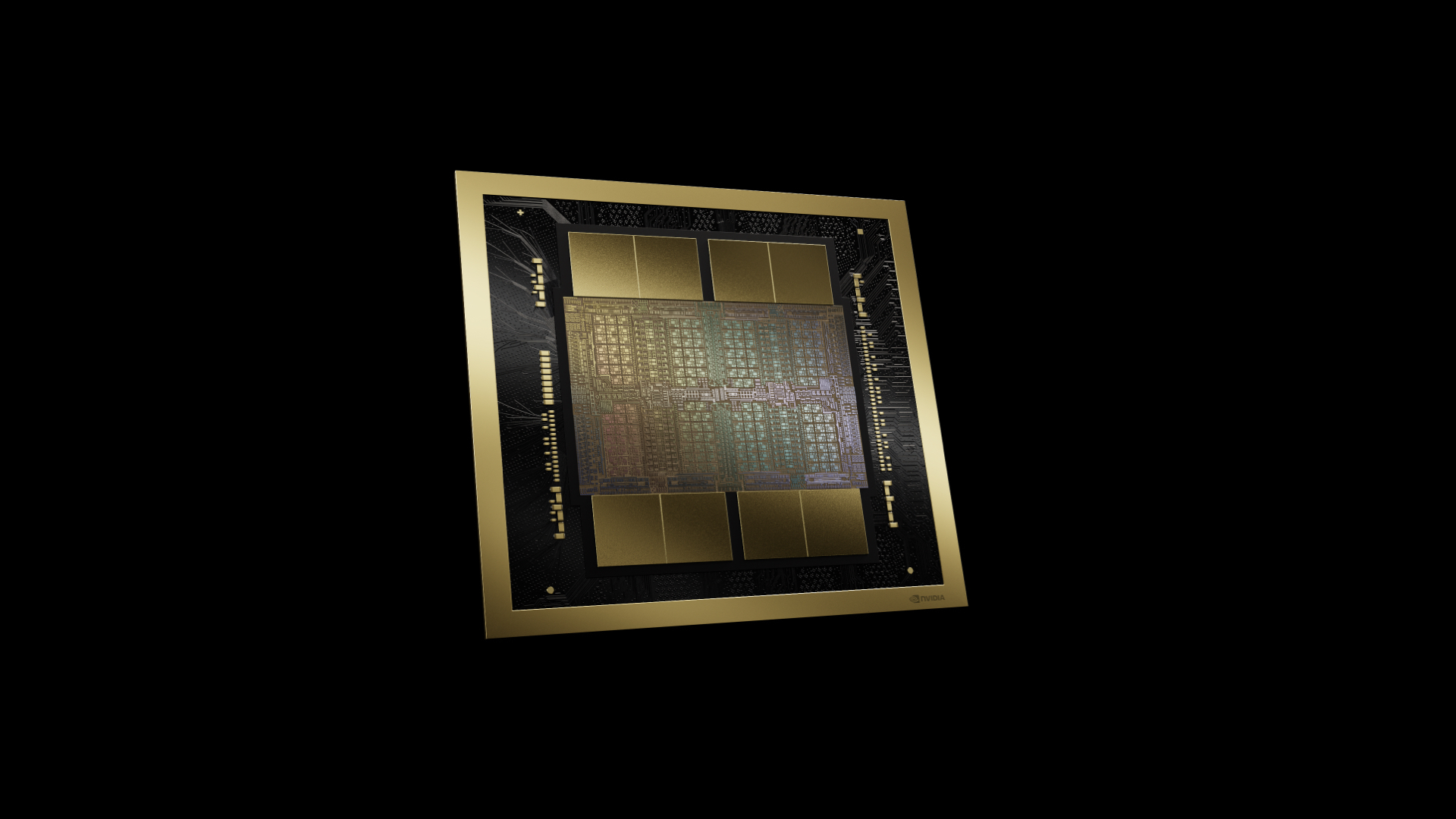
Nvidia shifts to CoWoS-L packaging for Blackwell GPU production ramp-up

As Nvidia ramps up production of its multi-chiplet Blackwell-series products, the company will use more CoWoS-L packaging capacity and less CoWoS-S packaging capacity, the company’s chief executive Jensen Huang confirmed at a press conference in Taiwan.
“As we move into Blackwell, we will use largely CoWoS-L,” said Huang at a press conference dedicated to the official opening of an advanced packaging facility by Siliconware Precision Industries Limited (SPIL), a subsidiary of ASE Technology, reports Reuters. “Of course, we are still manufacturing Hopper, and Hopper will use CowoS-S. We will also transition the CoWoS-S capacity to CoWoS-L. So it is not about reducing capacity. It’s actually increasing capacity into CoWoS-L.”
TSMC’s CoWoS-S is a high-end 2.5D packaging technology that uses a silicon interposer to connect chiplets in a system-in-package. This technology has been good enough for Nvidia’s Ampere-based A100 and Hopper-based H100 GPUs (as well as their derivatives) that connect to high-bandwidth memory (HBM). However, based on the Blackwell architecture, Nvidia’s B100 and B200 GPUs require two compute chiplets that need interconnection with 10 TB/s of bandwidth. This is enabled by TSMC’s CoWoS-L technology, which uses local silicon interconnect (LSI) bridges and an organic interposer that acts as a redistribution layer (RDL).
Nvidia’s B100 and B200 GPUs had a yield-killing design issue, which the company reportedly fixed by redesigning the top global routing metal layers and bumping out the Blackwell GPU silicon. As a result, the company can now produce GPUs with two compute dies at predictable yields.
However, to address the mass market, Nvidia is reportedly working on its B200A product featuring a monolithic B102 silicon with 144 GB (four stacks) of HBM3E and packaged using the proven CoWoS-S technology. This product is expected to have significantly lower performance than B100 and B200, but it will naturally be cheaper, too. However, unconfirmed rumors indicate that Nvidia intends to prioritize dual compute chiplet B100, B200, and eventually B300 GPUs over the alleged B200A.
It is important to note that SPIL, a subsidiary of ASE, is one of a few outsourced semiconductor assembly and test (OSAT) providers that have licensed TSMC’s CoWoS-S technology and possess the necessary equipment to build system-in-packages like H100, H200, and the alleged B200A. Huang’s attendance at SPIL’s opening ceremony may indicate that the company plans to use this capacity for its products, potentially suggesting the focus is on a future product rather than a current-gen one. Assuming this refers to the alleged B200A, it is a likely candidate to use SPIL’s CoWoS-S capacity. Of course, this remains speculation at this point.
#Nvidia #shifts #CoWoSL #packaging #Blackwell #GPU #production #rampup
