Samsung to introduce backside power delivery with 2nm-class production node: Report
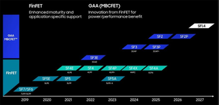
Although Samsung Foundry was the first chipmaker to adopt gate-all-around (GAA) transistors for its SF3E (3nm-class, early) fabrication technology, it will only adopt a backside power delivery network (BSPDN) starting from its SF2 (2nm-class) manufacturing process, according to a report from Chosun.com.
The report claims that promising results obtained with backside power delivery led to Samsung’s rethinking of implementing BSPDN into a commercial process technology. The company allegedly planned to introduce a backside power delivery network with its 1.7nm-class fabrication node but will pull it in and introduce it with the SF2 process due in 2025, based on the company’s roadmap. There is a major catch with the report, though: Samsung’s current public roadmap does not include any 1.7nm-class nodes and only contains SF2, SF2P, and SF1.4 technologies.
Samsung has implemented backside power delivery for two Arm-based test chips and achieved a 10% and 19% die area reduction without disclosing the process node, according to the company’s paper presented at the VLSI Symposium in mid-2023. Typically, backside power delivery enables thicker, lower-resistance wires, which can deliver more power to enable higher performance and save power. Samsung’s paper noted a 9.2% reduction in wiring length, enhancing performance. Additionally, the paper indicates that backside power delivery offers such benefits as a 3.6% Fmax improvement, a 2.4% standard block area reduction, and a 1.6% standard block performance improvement.
The work was not a part of Samsung’s and Arm’s ongoing collaboration to co-optimize Cortex-A and Cortex-C cores for Samsung’s SF2 (2nm-class) process technology, but given the results achieved by Samsung, it could end up being a major part of the project.
If the report is accurate, pulling in the introduction of a backside power delivery network to SF2 will make the process technology significantly more competitive against Intel’s 20A and 18A fabrication technologies in 2025, as well as TSMC’s N2P process in 2026 – 2027.
Meanwhile, the lack of BSDPN in SF3 and SF3P will certainly limit performance, power, and transistor density of these nodes compared to competing offerings. While lower peak performance, power, and transistor density may not be a huge disadvantage for some designs, it will inevitably be a drawback for things like smartphones and data center chips.
#Samsung #introduce #backside #power #delivery #2nmclass #production #node #Report

